





















HUAWEI Introduces Tau Scaling Law for Future Chips at the 2026 IEEE International Symposium
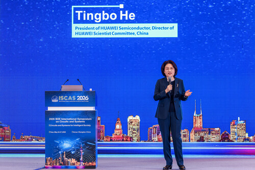
At the 2026 IEEE International Symposium on Circuits and
Systems in Shanghai, He Tingbo, President of HUAWEI's Semiconductor Business
Department, presented the Tau (τ) Scaling Law, a successor to Moore's Law for
guiding semiconductor development.
The new principle
replaces traditional geometric transistor scaling with time scaling as the core
measure of progress. The Tau Scaling Law reduces signal propagation delay and
system execution time to improve performance, energy efficiency and transistor
density.
For decades, the
semiconductor industry relied on shrinking transistors to increase computing
power and lower costs. However, continued scaling has become increasingly
difficult, while gains in cost-per-transistor and performance have slowed.
According to He,
the Tau Scaling Law offers an alternative path for semiconductor evolution with
HUAWEI developing technologies such as LogicFolding and a multi-level
optimization framework spanning devices, circuits, chips and systems.
The company aims to
reduce transistor and interconnect resistance and parasitic capacitance to
minimize physical-layer delay. At the circuit level, the LogicFolding
architecture restructures layouts to shorten critical signal paths, reducing
resistive and capacitive loads while improving transistor density and circuit
performance.
At the chip level,
HUAWEI applies coordinated software, architecture and silicon design to
optimize instruction and data flow, increasing parallelism and reducing
end-to-end execution time. At the system level, the company's UnifiedBus
interconnect protocol enables unified memory addressing and native memory
semantics for SuperPods, reducing communication latency across large-scale computing
systems.
He said HUAWEI has
applied the Tau Scaling Law to smartphones and AI computing. Over the past six
years, the company has designed and mass-produced 381 chips based on the new
framework for multiple industries and markets.
HUAWEI also revealed
that its Kirin processors scheduled for release in fall 2026 will be the first
chips to use the LogicFolding architecture, which will significantly improve
chip performance.
Tau Scaling Law is
also referred to as "Her's Law" named after He Tingbo by peers and
her colleagues.
HUAWEI projects
that by 2031 its high-end chips developed under the Tau Scaling framework could
achieve transistor densities comparable to 14-angstrom (1.4 nm) process
technologies.
He concluded by
emphasizing that collaboration will be essential for future progress, saying no
single company can solve the challenges of semiconductor evolution alone.
Leave A Comment